- 您现在的位置:买卖IC网 > Sheet目录369 > W971GG6JB25I (Winbond Electronics)IC DDR2 SDRAM 1GBIT 84WBGA
W971GG6JB
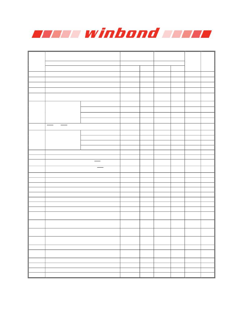
10.11.2 AC Characteristics and Operating Condition for -25/25L/25I/25A/25K/-3/-3A speed grades
Notes: 1-3 and 45-47 apply to the entire table
SYM.
SPEED GRADE
Bin(CL-t RCD -t RP)
DDR2-800
( -25/25L/25I/25A/25K )
5-5-5
DDR2-667
( -3/-3A )
5-5-5
UNITS 25 NOTES
PARAMETER
MIN.
MAX.
MIN.
MAX.
t RCD
t RP
t RC
t RAS
t RFC
Active to Read/Write Command Delay Time
Precharge to Active Command Period
Active to Ref/Active Command Period
Active to Precharge Command Period
Auto Refresh to Active/Auto Refresh command
period
-40°C ≤ T CASE ≤ 85°C*
12.5
12.5
52.5
40
127.5
?
?
?
?
70000
?
7.8
15
15
55
40
127.5
?
?
?
?
70000
?
7.8
nS
nS
nS
nS
nS
μ S
23
23
23
4,23
5
5
t REFI
Average periodic
refresh Interval
0°C ≤ T CASE ≤ 85°C
85°C < T CASE ≤ 95°C
95°C < T CASE ≤ 105°C*
?
?
?
7.8
3.9
3.9
?
?
?
7.8
3.9
?
μ S
μ S
μ S
5
5,6
5,6
t CCD
CAS to CAS command delay
2
?
2
?
n CK
t CK(avg) @ CL=3
5
8
5
8
nS
30,31
t CK(avg)
Average clock period
t CK(avg) @ CL=4
t CK(avg) @ CL=5
t CK(avg) @ CL=6
3.75
2.5
2.5
8
8
8
3.75
3
?
8
8
?
nS
nS
nS
30,31
30,31
30,31
t CH(avg)
t CL(avg)
t AC
t DQSCK
t DQSQ
t CKE
t RRD
t FAW
t WR
t DAL
t WTR
t RTP
t IS (base)
Average clock high pulse width
Average clock low pulse width
DQ output access time from CLK/ CLK
DQS output access time from CLK / CLK
DQS-DQ skew for DQS & associated DQ signals
CKE minimum high and low pulse width
Active to active command period for 2KB page size
Four Activate Window for 2KB page size
Write recovery time
Auto-precharge write recovery + precharge time
Internal Write to Read command delay
Internal Read to Precharge command delay
Address and control input setup time
0.45
0.45
-400
-350
?
3
10
45
15
WR + tn RP
7.5
7.5
175
0.55
0.55
400
350
200
?
?
?
?
?
?
?
?
0.45
0.45
-450
-400
?
3
10
50
15
WR + tn RP
7.5
7.5
200
0.55
0.55
450
400
240
?
?
?
?
?
?
?
?
t CK(avg)
t CK(avg)
pS
pS
pS
n CK
nS
nS
nS
n CK
nS
nS
pS
30,31
30,31
35
35
13
7
8,23
23
23
24
9,23
4,23
10,26,
40,42,43
t IH (base) Address and control input hold time
250
?
275
?
pS
11,26,
40,42,43
t IS (ref)
t IH (ref)
t IPW
t DQSS
t DSS
t DSH
t DQSH
t DQSL
Address and control input setup time
Address and control input hold time
Address and control input pulse width for each input
DQS latching rising transitions to associated clock
edges
DQS falling edge to CLK setup time
DQS falling edge hold time from CLK
DQS input high pulse width
DQS input low pulse width
375
375
0.6
-0.25
0.2
0.2
0.35
0.35
?
?
?
0.25
?
?
?
?
400
400
0.6
-0.25
0.2
0.2
0.35
0.35
?
?
?
0.25
?
?
?
?
pS
pS
t CK(avg)
t CK(avg)
t CK(avg)
t CK(avg)
t CK(avg)
t CK(avg)
10,26,
40,42,43
11,26,
40,42,43
28
28
28
* -40°C ≤ T CASE ≤ 85°C is for 25I/25A/25K/-3A grade only, 95°C < T CASE ≤ 105°C is for 25K grade only.
Publication Release Date: Sep. 24, 2013
- 45 -
Revision A09
发布紧急采购,3分钟左右您将得到回复。
相关PDF资料
W971GG8JB-25
IC DDR2 SDRAM 1GBIT 60WBGA
W9725G6IB-25
IC DDR2-800 SDRAM 256MB 84-WBGA
W9725G6JB25I
IC DDR2 SDRAM 256MBIT 84WBGA
W9725G6KB-25I
IC DDR2 SDRAM 256MBIT 84WBGA
W972GG6JB-3I
IC DDR2 SDRAM 2GBITS 84WBGA
W9751G6IB-25
IC DDR2-800 SDRAM 512MB 84-WBGA
W9751G6KB-25
IC DDR2 SDRAM 512MBIT 84WBGA
W9812G6JH-6I
IC SDRAM 128MBIT 54TSOPII
相关代理商/技术参数
W971GG6JB-25I
制造商:Winbond Electronics 功能描述:-40~85 1GB DDR2 FOR INDUSTRY
W971GG6JB25ITR
制造商:Winbond Electronics Corp 功能描述:1G, DDR2-800, X16, IND TEMP
W971GG6JB25TR
制造商:Winbond Electronics Corp 功能描述:NR, DDR2-800, X16
W971GG6JB-3
制造商:Winbond Electronics Corp 功能描述:1GBIT DDRII
W971GG6KB-18
制造商:Winbond Electronics Corp 功能描述:1G, DDR2-1066, X16 制造商:Winbond Electronics Corp 功能描述:IC MEMORY
W971GG8JB
制造商:WINBOND 制造商全称:Winbond 功能描述:16M × 8 BANKS × 8 BIT DDR2 SDRAM
W971GG8JB-25
功能描述:IC DDR2 SDRAM 1GBIT 60WBGA RoHS:是 类别:集成电路 (IC) >> 存储器 系列:- 标准包装:72 系列:- 格式 - 存储器:RAM 存储器类型:SRAM - 同步 存储容量:4.5M(256K x 18) 速度:133MHz 接口:并联 电源电压:3.135 V ~ 3.465 V 工作温度:0°C ~ 70°C 封装/外壳:100-LQFP 供应商设备封装:100-TQFP(14x20) 包装:托盘
W9725G6IB-25
功能描述:IC DDR2-800 SDRAM 256MB 84-WBGA RoHS:是 类别:集成电路 (IC) >> 存储器 系列:- 标准包装:1,000 系列:- 格式 - 存储器:EEPROMs - 串行 存储器类型:EEPROM 存储容量:4K (512 x 8) 速度:400kHz 接口:I²C,2 线串口 电源电压:2.7 V ~ 5.5 V 工作温度:-40°C ~ 85°C 封装/外壳:8-SOIC(0.173",4.40mm 宽) 供应商设备封装:8-MFP 包装:带卷 (TR)
