- 您现在的位置:买卖IC网 > Sheet目录369 > W971GG6JB25I (Winbond Electronics)IC DDR2 SDRAM 1GBIT 84WBGA
�� �
�
�W971GG6JB�
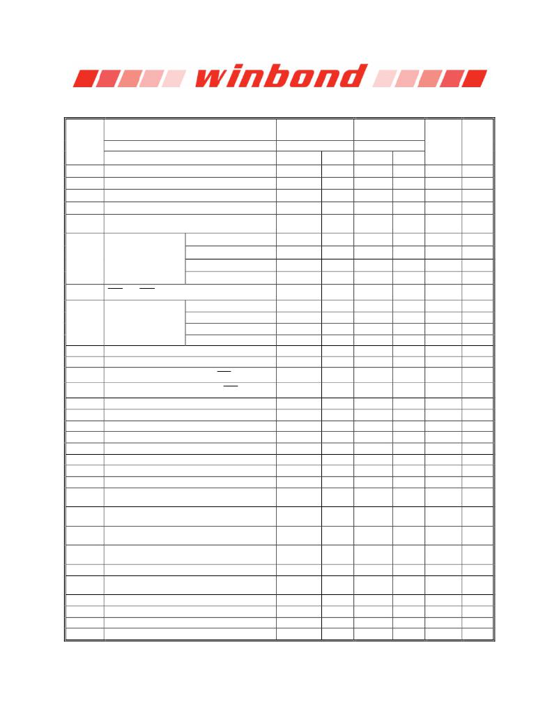
�10.11.2� AC� Characteristics� and� Operating� Condition� for� -25/25L/25I/25A/25K/-3/-3A� speed� grades�
�Notes:� 1-3� and� 45-47� apply� to� the� entire� table�
�SYM.�
�SPEED� GRADE�
�Bin(CL-t� RCD� -t� RP)�
�DDR2-800�
�(� -25/25L/25I/25A/25K� )�
�5-5-5�
�DDR2-667�
�(� -3/-3A� )�
�5-5-5�
�UNITS� 25� NOTES�
�PARAMETER�
�MIN.�
�MAX.�
�MIN.�
�MAX.�
�t� RCD�
�t� RP�
�t� RC�
�t� RAS�
�t� RFC�
�Active� to� Read/Write� Command� Delay� Time�
�Precharge� to� Active� Command� Period�
�Active� to� Ref/Active� Command� Period�
�Active� to� Precharge� Command� Period�
�Auto� Refresh� to� Active/Auto� Refresh� command�
�period�
�-40°C� ≤� T� CASE� ≤� 85°C*�
�12.5�
�12.5�
�52.5�
�40�
�127.5�
�?�
�?�
�?�
�?�
�70000�
�?�
�7.8�
�15�
�15�
�55�
�40�
�127.5�
�?�
�?�
�?�
�?�
�70000�
�?�
�7.8�
�nS�
�nS�
�nS�
�nS�
�nS�
�μ� S�
�23�
�23�
�23�
�4,23�
�5�
�5�
�t� REFI�
�Average� periodic�
�refresh� Interval�
�0°C� ≤� T� CASE� ≤� 85°C�
�85°C� <� T� CASE� ≤� 95°C�
�95°C� <� T� CASE� ≤� 105°C*�
�?�
�?�
�?�
�7.8�
�3.9�
�3.9�
�?�
�?�
�?�
�7.8�
�3.9�
�?�
�μ� S�
�μ� S�
�μ� S�
�5�
�5,6�
�5,6�
�t� CCD�
�CAS� to� CAS� command� delay�
�2�
�?�
�2�
�?�
�n� CK�
�t� CK(avg)� @� CL=3�
�5�
�8�
�5�
�8�
�nS�
�30,31�
�t� CK(avg)�
�Average� clock� period�
�t� CK(avg)� @� CL=4�
�t� CK(avg)� @� CL=5�
�t� CK(avg)� @� CL=6�
�3.75�
�2.5�
�2.5�
�8�
�8�
�8�
�3.75�
�3�
�?�
�8�
�8�
�?�
�nS�
�nS�
�nS�
�30,31�
�30,31�
�30,31�
�t� CH(avg)�
�t� CL(avg)�
�t� AC�
�t� DQSCK�
�t� DQSQ�
�t� CKE�
�t� RRD�
�t� FAW�
�t� WR�
�t� DAL�
�t� WTR�
�t� RTP�
�t� IS� (base)�
�Average� clock� high� pulse� width�
�Average� clock� low� pulse� width�
�DQ� output� access� time� from� CLK/� CLK�
�DQS� output� access� time� from� CLK� /� CLK�
�DQS-DQ� skew� for� DQS� &� associated� DQ� signals�
�CKE� minimum� high� and� low� pulse� width�
�Active to active command period for 2KB page size�
�Four� Activate� Window� for� 2KB� page� size�
�Write� recovery� time�
�Auto-precharge� write� recovery� +� precharge� time�
�Internal� Write� to� Read� command� delay�
�Internal� Read� to� Precharge� command� delay�
�Address� and� control� input� setup� time�
�0.45�
�0.45�
�-400�
�-350�
�?�
�3�
�10�
�45�
�15�
�WR� +� tn� RP�
�7.5�
�7.5�
�175�
�0.55�
�0.55�
�400�
�350�
�200�
�?�
�?�
�?�
�?�
�?�
�?�
�?�
�?�
�0.45�
�0.45�
�-450�
�-400�
�?�
�3�
�10�
�50�
�15�
�WR + tn� RP�
�7.5�
�7.5�
�200�
�0.55�
�0.55�
�450�
�400�
�240�
�?�
�?�
�?�
�?�
�?�
�?�
�?�
�?�
�t� CK(avg)�
�t� CK(avg)�
�pS�
�pS�
�pS�
�n� CK�
�nS�
�nS�
�nS�
�n� CK�
�nS�
�nS�
�pS�
�30,31�
�30,31�
�35�
�35�
�13�
�7�
�8,23�
�23�
�23�
�24�
�9,23�
�4,23�
�10,26,�
�40,42,43�
�t� IH� (base)� Address� and� control� input� hold� time�
�250�
�?�
�275�
�?�
�pS�
�11,26,�
�40,42,43�
�t� IS� (ref)�
�t� IH� (ref)�
�t� IPW�
�t� DQSS�
�t� DSS�
�t� DSH�
�t� DQSH�
�t� DQSL�
�Address� and� control� input� setup� time�
�Address� and� control� input� hold� time�
�Address and control input pulse width for each input�
�DQS� latching� rising� transitions� to� associated� clock�
�edges�
�DQS� falling� edge� to� CLK� setup� time�
�DQS� falling� edge� hold� time� from� CLK�
�DQS� input� high� pulse� width�
�DQS� input� low� pulse� width�
�375�
�375�
�0.6�
�-0.25�
�0.2�
�0.2�
�0.35�
�0.35�
�?�
�?�
�?�
�0.25�
�?�
�?�
�?�
�?�
�400�
�400�
�0.6�
�-0.25�
�0.2�
�0.2�
�0.35�
�0.35�
�?�
�?�
�?�
�0.25�
�?�
�?�
�?�
�?�
�pS�
�pS�
�t� CK(avg)�
�t� CK(avg)�
�t� CK(avg)�
�t� CK(avg)�
�t� CK(avg)�
�t� CK(avg)�
�10,26,�
�40,42,43�
�11,26,�
�40,42,43�
�28�
�28�
�28�
�*� -40°C� ≤� T� CASE� ≤� 85°C� is� for� 25I/25A/25K/-3A� grade� only,� 95°C� <� T� CASE� ≤� 105°C� is� for� 25K� grade� only.�
�Publication� Release� Date:� Sep.� 24,� 2013�
�-� 45� -�
�Revision� A09�
�发布紧急采购,3分钟左右您将得到回复。
相关PDF资料
W971GG8JB-25
IC DDR2 SDRAM 1GBIT 60WBGA
W9725G6IB-25
IC DDR2-800 SDRAM 256MB 84-WBGA
W9725G6JB25I
IC DDR2 SDRAM 256MBIT 84WBGA
W9725G6KB-25I
IC DDR2 SDRAM 256MBIT 84WBGA
W972GG6JB-3I
IC DDR2 SDRAM 2GBITS 84WBGA
W9751G6IB-25
IC DDR2-800 SDRAM 512MB 84-WBGA
W9751G6KB-25
IC DDR2 SDRAM 512MBIT 84WBGA
W9812G6JH-6I
IC SDRAM 128MBIT 54TSOPII
相关代理商/技术参数
W971GG6JB-25I
制造商:Winbond Electronics 功能描述:-40~85 1GB DDR2 FOR INDUSTRY
W971GG6JB25ITR
制造商:Winbond Electronics Corp 功能描述:1G, DDR2-800, X16, IND TEMP
W971GG6JB25TR
制造商:Winbond Electronics Corp 功能描述:NR, DDR2-800, X16
W971GG6JB-3
制造商:Winbond Electronics Corp 功能描述:1GBIT DDRII
W971GG6KB-18
制造商:Winbond Electronics Corp 功能描述:1G, DDR2-1066, X16 制造商:Winbond Electronics Corp 功能描述:IC MEMORY
W971GG8JB
制造商:WINBOND 制造商全称:Winbond 功能描述:16M × 8 BANKS × 8 BIT DDR2 SDRAM
W971GG8JB-25
功能描述:IC DDR2 SDRAM 1GBIT 60WBGA RoHS:是 类别:集成电路 (IC) >> 存储器 系列:- 标准包装:72 系列:- 格式 - 存储器:RAM 存储器类型:SRAM - 同步 存储容量:4.5M(256K x 18) 速度:133MHz 接口:并联 电源电压:3.135 V ~ 3.465 V 工作温度:0°C ~ 70°C 封装/外壳:100-LQFP 供应商设备封装:100-TQFP(14x20) 包装:托盘
W9725G6IB-25
功能描述:IC DDR2-800 SDRAM 256MB 84-WBGA RoHS:是 类别:集成电路 (IC) >> 存储器 系列:- 标准包装:1,000 系列:- 格式 - 存储器:EEPROMs - 串行 存储器类型:EEPROM 存储容量:4K (512 x 8) 速度:400kHz 接口:I²C,2 线串口 电源电压:2.7 V ~ 5.5 V 工作温度:-40°C ~ 85°C 封装/外壳:8-SOIC(0.173",4.40mm 宽) 供应商设备封装:8-MFP 包装:带卷 (TR)